Kazakhstan, Almaty, Almaly district, Nursultan Nazarbayev avenue, house 65, office 503
Mn - Fr: 9:00 - 21:00
Call me
Equipment
We perform the following types of PCB mounting
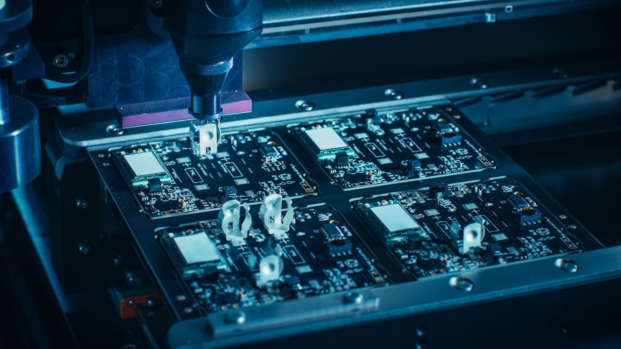
SMD installation
Surface mounting of printed circuit boards is the installation of components on the surface of the board by soldering the SMD component to the contact pad. Advantages:
- the possibility of manufacturing double-sided boards
- the absence of the usual conclusions reduces their size and weight
- increasing the density of the layout due to the small size of the electric elements
- improving electrical parameters due to the layout
- facilitating the repair of boards, it is easier to clean the contact pads from the flux
- the process is easy to automate
- reducing the cost of products in mass production

Manual DIP installation
Output mounting of printed circuit boards is the installation of electronic components, in which the terminals of the elements pass through the through holes of the board. The contacts are soldered to the metallized layer in the holes and firmly fixed in them. Advantages:
- allows you to mount boards of any complexity
reliable solder of all contacts in metallized holes - reduced risk of overheating of components, their damage and peeling
- the possibility of soldering leads to the inner layers of the plate
- eliminates machine defects associated with unforeseen depletion of supplies of consumables
Thank you! The form has been sent!
Contact information
Kazakhstan, Almaty, Nursultan Nazarbayev avenue, house 65, office 503
Monday - Friday 9:00 to 21:00
Copyright © 2020

Thanks! The form has been sent